




 Home
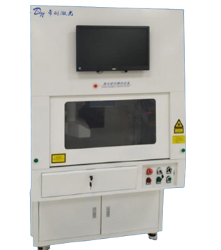
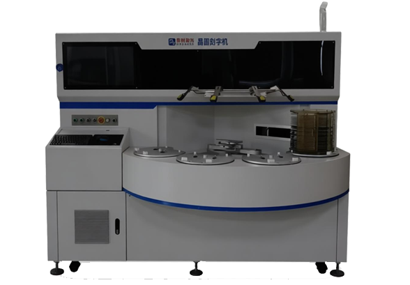
HomeWafer soft (hard) engraving machine
Focused on the industry for 8 years, Denai Laser focuses on expertise
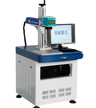
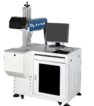
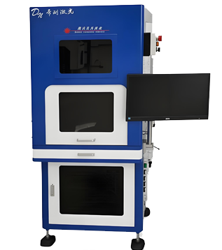
The laser acts on the wafer, instantly ablating and vaporizing it through a thermal light source or breaking the molecular bonds of the material through a cold light source, leaving corresponding characters, text, or patterns on the wafer surface. Wafer marking features automatic loading and unloading, automatic positioning, and automatic marking functions.
价格咨询 >>
 Porducts
-
Plastic laser welding machine- Trajectory laser welding plastic machine - Quasi synchronous laser welding plastic machine - Deep penetration laser plastic welding equipment - Cylindrical plastic laser welding machine - Laser axial plastic welding machine - Transparent material plastic welding machine - Synchronous plastic laser welding machine - Bumper laser cutting and welding integrated machine
-
Laser engraving machine
-
Full-field laser cleaning machine
-
Precision laser cutting machine
留言咨询
Product OverviewThe laser acts on the wafer, instantly thermally ablating and vaporizing it through a thermal light source or breaking the molecular bonds of the material through a cold light source, leaving corresponding characters, text, or patterns on the wafer surface. Wafer marking features automatic loading and unloading, automatic positioning, and automatic marking functions.
Features of the equipment
◆CCD automatic precise positioning;◆ Automatic film retrieval and placement by robotic arm;
◆ Both the front and back sides can be marked;
◆ Professional dust removal system;
◆ Automatic counting;
◆ Automatic film jumping in case of empty material. (Optional)
◆Number of cards (optional)
Product parametersName | parameter value | |
Marking format | Hard marking | Soft marking |
ay | 100W | 20W |
Marking depth(mm) | 3.-60um | 2-5um |
Marking speed(mm/s) | ≤7000mm | |
Wafer processing dimensions | 2”-12” | |
Position accuracy | ±0.1mm | |
font standard | SEMI | |
Industrial gas source(L/min) | 0.6 | |
Capacity cycle | ≥100片/H | |
Machine power(KVA) | 2.5KW | 1.5KW |
Dust removal standards | 0.3μm particle | |
Application Areas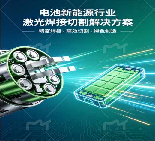
Laser welding and cutting solutions in the field of battery new energy industry
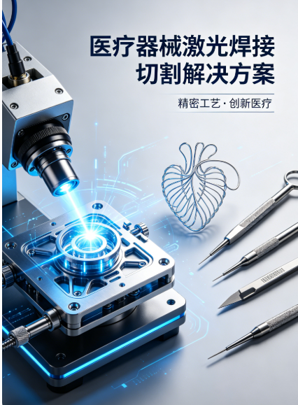
Laser welding and cutting solutions in the medical device industry
Laser Welding and Cutting Integrated Solution for Plastic Packaging Industry
Laser cutting and welding solutions for the semiconductor industry
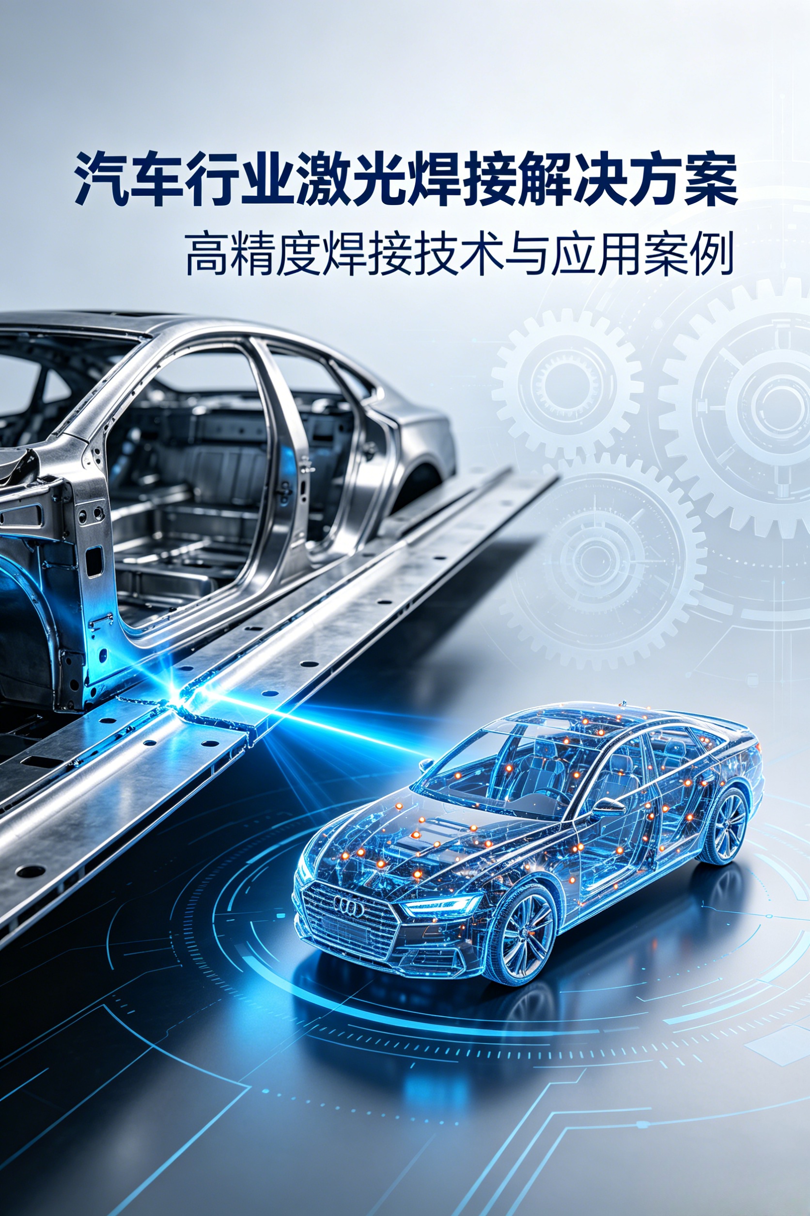
Laser welding solutions for the automotive industry
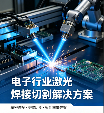
Laser welding and cutting solutions for the electronics industry
Sample Display