





Laser cutting and welding solutions for the semiconductor industry
 Home
Home
Dine Laser has developed a complete and directly implementable solution for laser cutting (wafer/hard and brittle materials) and laser welding (packaging/power modules) in the semiconductor industry, covering: process route + equipment selection + key parameters + yield/efficiency indicators + typical cases + risk control.
1. Semiconductor laser cutting solution (wafer / third-generation semiconductor)
(1) Core pain points
Silicon / Ultra-thin Silicon (20–50μm): Large chipping edges during mechanical cutting, prone to fracturing, and thermal damage
SiC/GaN (hard and brittle): chipping 5–15μm, low yield, high cost
Low-K / ultra-thin wafer: heat-sensitive, prone to interlayer cracking
(II) Material-specific Process Plan
1) Silicon wafer (6–12 inches, 20–200μm)
Recommended process: UV/Picosecond laser stealth dicing
Laser: 355nm UV / 532nm green picosecond, 10–50W
Core parameters:
Cutting track: 10–20μm (traditional blade 30–50μm)
Chipping: <1μm (traditional 5–15μm)
Heat-affected zone: <5μm
Yield: 99.5%–99.9%
Process: Material loading → Visual positioning → Invisible cutting (internal modification) → Splitting → Cleaning → Material unloading
Applicable to: ultra-thin wafers, WLP, power devices (MOSFET/IGBT)
2) SiC/GaN third-generation semiconductor (6–8 inches)
Recommended process: UV laser slotting + invisible cutting
Laser: 355nm ultraviolet, 20–100W; or femtosecond laser
Core parameters:
Chipping: ≤2μm (reduced by 80%)
Slot depth: 5–20μm, accuracy ±1μm
Yield: 99.0%–99.5%
Efficiency: ↑30%+
Application: Power devices for new energy vehicles, 5G RF chips
3) Low-K / Ultra-thin Wafer (<50μm)
Recommended process: picosecond ultraviolet laser cold ablation
Advantages: No thermal damage, no delamination, smooth edges
Kerf: 5–15μm, Ra<1μm
(III) Standard equipment configuration (mass production line)
Complete machine: Fully automatic wafer laser cutting machine (marble base + high-precision platform)
Motion positioning: ±0.5μm, repeatability ±0.1μm
Vision: Dual CCD + AI vision (automatic edge detection, alignment, and inspection)
Auxiliary: automatic loading and unloading, protective liquid coating, cleaning and drying
Representative models: Han's DA100, Huagong Dicing Agent, DISCO DFL7360
(IV) Typical Cases (Mass Production Data)
Case 1: Cutting of 8-inch ultra-thin silicon (35μm)
Process: 15W UV invisible cutting
Production capacity: 120 pieces/hour
Yield: 99.7% (traditional blade: 92%)
Edge chipping: <0.8μm
Case 2: 6-inch SiC slotting
Process: 50W UV laser
Slot width: 15μm, depth: 10μm
Yield: 99.2%
Efficiency: ↑40%
II. Semiconductor laser welding solutions (packaging/power modules)
(1) Core pain points
Fine pitch packaging (less than 0.25mm): traditional soldering is prone to bridge connection and poor soldering
Power module (IGBT/SiC): dissimilar materials of copper and aluminum, high heat dissipation requirements
Thermal sensor (MEMS/sensor): Highly susceptible to thermal effects and prone to failure
(II) Process schemes for different scenarios
1) Precision interconnection (Chiplet/2.5D/3D packaging)
Applications: Chip bump-substrate, solder ball bonding, ultra-fine leads
Recommended process: UV laser solder ball bonding / spot welding
Laser: 355nm UV, 10–50W; pulsed fiber laser
Core parameters:
Solder joint diameter: 50–100μm
Heat-affected zone: <0.2mm
Positioning accuracy: ±1μm
Yield: 99.7%–99.9%
Applicable to: AI chips, high-speed optical modules, MEMS
2) Power module soldering (IGBT/SiC)
Application: DBC copper clad laminate - copper PIN, copper-aluminum heat dissipation structure
Recommended process: Blue light / fiber laser welding (high copper absorption rate)
Laser: 450nm blue light (500–1500W) / 1064nm fiber
Core parameters:
Penetration depth: copper ≥ 5mm, aluminum ≥ 3mm
No splashes, no pores
Yield: ≥99.99%
Application: electric control of new energy vehicles, photovoltaic inverters
3) Sealing/Hermetic welding (sensors/optical components)
Application: Metal housing (Kovar / stainless steel), ceramic-metal packaging
Recommended process: Pulsed fiber laser seam welding
Core parameters:
Weld width: 0.3–0.8mm
Tightness: ≤1×10⁻⁹ Pa・m³/s
Yield: 99.5%+
(III) Standard equipment configuration (mass production line)
Complete machine: Precision laser welding machine (marble base + constant temperature control)
Motion positioning: ±1μm, high-speed galvanometer (scanning speed ≥2m/s)
Vision: 3D vision + real-time molten pool monitoring + AI closed-loop temperature control
Auxiliary: Nitrogen protection, automatic solder ball feeding, automatic loading and unloading
Representative model: DiNai semiconductor soldering station
(IV) Typical Cases (Mass Production Data)
Case 1: IGBT module PIN pin welding
Process: 300W fiber laser spot welding
Weld spot: φ0.5mm, penetration depth 0.8mm
Yield: 99.99%
Production capacity: 3000 units/hour
Case 2: Micro LED High-Volume Bonding
Process: Infrared laser linear spot
Positioning accuracy: ±1.5μm
Yield: 99.99%
Production capacity: 100,000 pieces/hour
III. Comparison of Overall Scheme Advantages (vs Traditional Process)
Laser cutting vs mechanical blade
Kerf: 10–20μm vs 30–50μm (material saving 3–5 times)
Edge chipping: <1μm vs 5–15μm
Thermal impact: <5μm vs mechanical stress + high temperature
Yield: 99.5%+ vs 85%-92%
Efficiency: ↑30%–100%
Laser welding vs soldering / brazing
Thermal impact: <0.2mm vs 2–5mm
Accuracy: ±1μm vs ±50μm
Dissimilar materials: copper / aluminum / ceramic weldable vs difficult
Yield: 99.7%+ vs 95%-98%
Automation: easy to integrate vs difficult
IV. Selection Suggestions (By Process)
Cutting selection
Ultra-thin silicon (<50μm): UV invisible cutting
SiC/GaN: UV femtosecond grooving + invisible cutting
Ordinary silicon (≥100μm): Green laser / Fiber laser cutting
Welding selection
Fine pitch packaging: UV laser solder ball bonding
Power module (copper): Blue laser welding
Airtight sealing cover: Pulsed fiber laser seam welding
V. Risk control and yield assurance
Environment: Constant temperature (±0.5℃), dust-free (Class 1000), shock-resistant
Process: AI parameter library + real-time monitoring + closed-loop feedback
Optics: Regularly calibrate the optical path, clean the lenses, and stabilize the power
Inspection: AI vision automatically inspects for chipping, cracks, and soldering defects
1. Semiconductor laser cutting solution (wafer / third-generation semiconductor)
(1) Core pain points
Silicon / Ultra-thin Silicon (20–50μm): Large chipping edges during mechanical cutting, prone to fracturing, and thermal damage
SiC/GaN (hard and brittle): chipping 5–15μm, low yield, high cost
Low-K / ultra-thin wafer: heat-sensitive, prone to interlayer cracking
(II) Material-specific Process Plan
1) Silicon wafer (6–12 inches, 20–200μm)
Recommended process: UV/Picosecond laser stealth dicing
Laser: 355nm UV / 532nm green picosecond, 10–50W
Core parameters:
Cutting track: 10–20μm (traditional blade 30–50μm)
Chipping: <1μm (traditional 5–15μm)
Heat-affected zone: <5μm
Yield: 99.5%–99.9%
Process: Material loading → Visual positioning → Invisible cutting (internal modification) → Splitting → Cleaning → Material unloading
Applicable to: ultra-thin wafers, WLP, power devices (MOSFET/IGBT)
2) SiC/GaN third-generation semiconductor (6–8 inches)
Recommended process: UV laser slotting + invisible cutting
Laser: 355nm ultraviolet, 20–100W; or femtosecond laser
Core parameters:
Chipping: ≤2μm (reduced by 80%)
Slot depth: 5–20μm, accuracy ±1μm
Yield: 99.0%–99.5%
Efficiency: ↑30%+
Application: Power devices for new energy vehicles, 5G RF chips
3) Low-K / Ultra-thin Wafer (<50μm)
Recommended process: picosecond ultraviolet laser cold ablation
Advantages: No thermal damage, no delamination, smooth edges
Kerf: 5–15μm, Ra<1μm
(III) Standard equipment configuration (mass production line)
Complete machine: Fully automatic wafer laser cutting machine (marble base + high-precision platform)
Motion positioning: ±0.5μm, repeatability ±0.1μm
Vision: Dual CCD + AI vision (automatic edge detection, alignment, and inspection)
Auxiliary: automatic loading and unloading, protective liquid coating, cleaning and drying
Representative models: Han's DA100, Huagong Dicing Agent, DISCO DFL7360
(IV) Typical Cases (Mass Production Data)
Case 1: Cutting of 8-inch ultra-thin silicon (35μm)
Process: 15W UV invisible cutting
Production capacity: 120 pieces/hour
Yield: 99.7% (traditional blade: 92%)
Edge chipping: <0.8μm
Case 2: 6-inch SiC slotting
Process: 50W UV laser
Slot width: 15μm, depth: 10μm
Yield: 99.2%
Efficiency: ↑40%
II. Semiconductor laser welding solutions (packaging/power modules)
(1) Core pain points
Fine pitch packaging (less than 0.25mm): traditional soldering is prone to bridge connection and poor soldering
Power module (IGBT/SiC): dissimilar materials of copper and aluminum, high heat dissipation requirements
Thermal sensor (MEMS/sensor): Highly susceptible to thermal effects and prone to failure
(II) Process schemes for different scenarios
1) Precision interconnection (Chiplet/2.5D/3D packaging)
Applications: Chip bump-substrate, solder ball bonding, ultra-fine leads
Recommended process: UV laser solder ball bonding / spot welding
Laser: 355nm UV, 10–50W; pulsed fiber laser
Core parameters:
Solder joint diameter: 50–100μm
Heat-affected zone: <0.2mm
Positioning accuracy: ±1μm
Yield: 99.7%–99.9%
Applicable to: AI chips, high-speed optical modules, MEMS
2) Power module soldering (IGBT/SiC)
Application: DBC copper clad laminate - copper PIN, copper-aluminum heat dissipation structure
Recommended process: Blue light / fiber laser welding (high copper absorption rate)
Laser: 450nm blue light (500–1500W) / 1064nm fiber
Core parameters:
Penetration depth: copper ≥ 5mm, aluminum ≥ 3mm
No splashes, no pores
Yield: ≥99.99%
Application: electric control of new energy vehicles, photovoltaic inverters
3) Sealing/Hermetic welding (sensors/optical components)
Application: Metal housing (Kovar / stainless steel), ceramic-metal packaging
Recommended process: Pulsed fiber laser seam welding
Core parameters:
Weld width: 0.3–0.8mm
Tightness: ≤1×10⁻⁹ Pa・m³/s
Yield: 99.5%+
(III) Standard equipment configuration (mass production line)
Complete machine: Precision laser welding machine (marble base + constant temperature control)
Motion positioning: ±1μm, high-speed galvanometer (scanning speed ≥2m/s)
Vision: 3D vision + real-time molten pool monitoring + AI closed-loop temperature control
Auxiliary: Nitrogen protection, automatic solder ball feeding, automatic loading and unloading
Representative model: DiNai semiconductor soldering station
(IV) Typical Cases (Mass Production Data)
Case 1: IGBT module PIN pin welding
Process: 300W fiber laser spot welding
Weld spot: φ0.5mm, penetration depth 0.8mm
Yield: 99.99%
Production capacity: 3000 units/hour
Case 2: Micro LED High-Volume Bonding
Process: Infrared laser linear spot
Positioning accuracy: ±1.5μm
Yield: 99.99%
Production capacity: 100,000 pieces/hour
III. Comparison of Overall Scheme Advantages (vs Traditional Process)
Laser cutting vs mechanical blade
Kerf: 10–20μm vs 30–50μm (material saving 3–5 times)
Edge chipping: <1μm vs 5–15μm
Thermal impact: <5μm vs mechanical stress + high temperature
Yield: 99.5%+ vs 85%-92%
Efficiency: ↑30%–100%
Laser welding vs soldering / brazing
Thermal impact: <0.2mm vs 2–5mm
Accuracy: ±1μm vs ±50μm
Dissimilar materials: copper / aluminum / ceramic weldable vs difficult
Yield: 99.7%+ vs 95%-98%
Automation: easy to integrate vs difficult
IV. Selection Suggestions (By Process)
Cutting selection
Ultra-thin silicon (<50μm): UV invisible cutting
SiC/GaN: UV femtosecond grooving + invisible cutting
Ordinary silicon (≥100μm): Green laser / Fiber laser cutting
Welding selection
Fine pitch packaging: UV laser solder ball bonding
Power module (copper): Blue laser welding
Airtight sealing cover: Pulsed fiber laser seam welding
V. Risk control and yield assurance
Environment: Constant temperature (±0.5℃), dust-free (Class 1000), shock-resistant
Process: AI parameter library + real-time monitoring + closed-loop feedback
Optics: Regularly calibrate the optical path, clean the lenses, and stabilize the power
Inspection: AI vision automatically inspects for chipping, cracks, and soldering defects
Popular Products
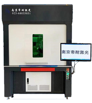
Semiconductor field
Trajectory laser welding plastic machine22
Learn more
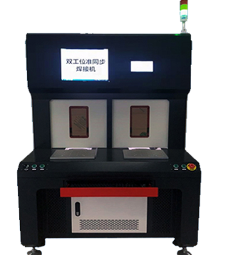
Semiconductor field
Quasi synchronous laser welding plastic machine22
Learn more
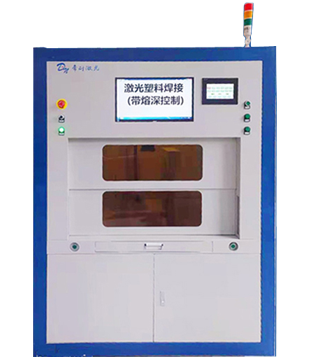
Semiconductor field
Deep penetration laser plastic welding equipment22
Learn more
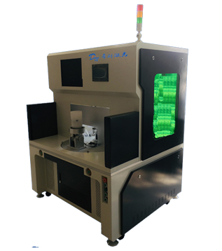
Semiconductor field
Cylindrical plastic laser welding machine22
Learn more
Semiconductor field
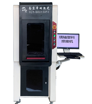
Laser axial plastic welding machine22
Learn more
Semiconductor field
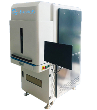
Transparent material plastic welding machine22
Learn more