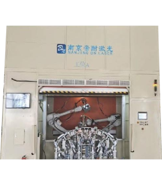





Laser welding and cutting solutions for the electronics industry
 Home
Home Laser welding and cutting solutions for the electronics industry
1. Industry Overview
Currently, electronic manufacturing is rapidly evolving towards miniaturization, high density, ultra-thinness, and high reliability. Traditional processing technologies for PCBs, FPCs, consumer electronic structural components, semiconductor packaging, and precision components face challenges such as high mechanical stress, high thermal damage, burr and edge chipping, low yield rates, and slow model changes. Laser processing, with its characteristics of non-contact, high precision, low thermal impact, no mechanical stress, and high automation, is suitable for core processes in the electronics industry such as precision welding, precision cutting, drilling, and trimming. It can solve the processing difficulties of thin materials, micro-parts, and high-precision electronic products that are difficult to handle with traditional processes, and is adaptable to both mass production and small-batch customized production.
II. Analysis of industry pain points
2.1 Welding pain points
The solder joints of precision components are tiny, and traditional soldering temperature is uncontrollable, which easily burns through the solder pads and damages surrounding components;
Welding of high-reflective materials such as copper and aluminum results in large spatter, blackened welding spots, and poor consistency;
FPC, shielding cases, and precision thin-walled spring pieces are prone to deformation, resulting in a high rate of poor quality issues such as solder joint failure and detachment;
Manual welding relies on proficiency, suffers from poor consistency in mass production, and incurs rising labor costs year by year.
2.2 Cutting pain points
Traditional milling cutters and die-cutting boards have high stress, and PCB boards are prone to microcracks, delamination, and edge chipping;
The cutting edge of the FPC flexible material die-cutting tool becomes hard, and it is prone to breaking when repeatedly bent, resulting in a short service life;
Ultra-thin glass, ceramic substrates, and wafer brittle materials are prone to edge chipping and cracking;
The cost of mold development is high, product iteration is slow, and irregular structures cannot be quickly adapted.
III. Overall Solution Design
3.1 Overall idea of the plan
Relying on fiber laser, ultraviolet laser, and picosecond micro-nano processing technology, coupled with CCD visual positioning, automatic fixtures, and closed-loop temperature control systems, we have established an integrated production line for precision laser welding and precision laser cutting. We customize process parameters for different electronic materials, thicknesses, and precision requirements, achieving stress-free processing, low-spatter welding, and smooth edges without burrs. The production line is suitable for a wide range of products, including PCBs, FPCs, consumer electronics structural components, semiconductor components, and battery precision components. It is compatible with automated loading and unloading, MES data traceability, and meets high-standard production requirements for mass production.
3.2 Core Process Solutions
(1) Laser welding solution
Utilizing pulsed fiber laser technology combined with annular spot optimization, precise control over heat input is achieved, narrowing the heat-affected zone. Customized welding processes are tailored for high-reflective metals and thin-walled precision components.
Welding of metal structural components: mobile phone mid-plane, nut studs, shielding covers, spring clips, connectors, ensuring uniform solder joints, stable tensile strength, and no deformation;
Circuit board soldering: PCB solder pads, FPC flexible board pins, gold-plated contacts, tiny solder joints, without burning the substrate or damaging the circuit;
Battery module welding: sealing welding of pole ears, busbars, and battery cases, with low spatter, strong sealing, and no leakage;
Dissimilar material welding: copper-aluminum, stainless steel + copper composite welding, addressing the issues of difficult fusion and susceptibility to cracking in dissimilar materials.
(2) Laser cutting solution
Utilizing UV cold laser technology combined with high-speed galvanometer cutting, the system generates minimal heat and operates without mechanical contact, making it suitable for cutting brittle materials, flexible materials, and ultra-thin plates.
PCB rigid board separation: automatic panel separation and cutting, no stress, no dust, no chipping, eliminating delamination and cracking in the later stage;
FPC flexible board cutting: contour cutting, slotting, window opening, with smooth cutting edges, resistant to bending, enhancing product service life;
Cutting of brittle materials: ultra-thin glass, ceramic substrates, semiconductor wafers, with flat cuts and edge chipping ≤1μm;
Special-shaped precision cutting: micro-sized special-shaped holes, narrow slots, precise contours, with a minimum cutting slit of up to 20μm.
IV. Equipment Configuration Plan
Process Type | Models | Laser type | Core configuration | Applicable Products |
|---|---|---|---|---|
Precision welding | Fully automatic laser welding machine | Fiber pulse laser | CCD vision, constant temperature control system, automatic fixture | Structural components, batteries, and component pins |
Precision cutting | UV laser cutting machine | UV cold laser | High-speed galvanometer, high-definition vision, dust removal system | PCB, FPC, thin film materials |
Micro-nano fabrication | Picosecond laser micro-machining machine | Picosecond laser | Ultra-high precision optical path, precision displacement platform | Glass, ceramics, semiconductor wafers |
V. Advantages of the Plan
1. Extremely high precision: positioning accuracy ±0.01mm, meeting the requirements of micron-level electronic precision machining;
2. Stable quality: no stress, low thermal damage, with a yield rate of over 99.5%;
3. High universality: No need for mold making, one-click import of drawings, and quick product switching;
4. High degree of automation: Equipped with automatic loading and unloading, it reduces manual intervention and labor costs;
5. Green production: Processing without dust and with minimal waste, meeting the standards of dust-free workshops in the electronics industry.
VI. Applicable Industries and Products
Consumer electronics, communication electronics, semiconductor packaging, new energy batteries, automotive electronics, precision components; covering products such as mobile phones, headphones, smart wearables, circuit boards, sensors, chip carriers, ceramic structural parts, etc.
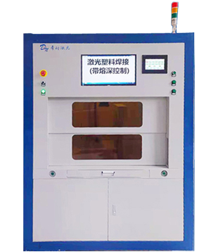
Deep penetration laser plastic welding equipment22
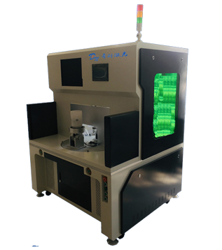
Cylindrical plastic laser welding machine22
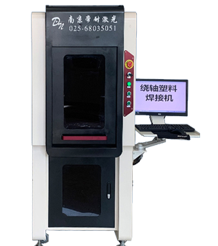
Laser axial plastic welding machine22
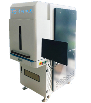
Transparent material plastic welding machine22
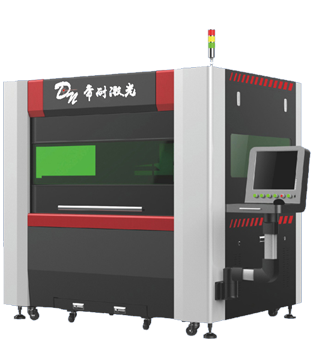
Synchronous plastic laser welding machine22